Photonics Packaging
Exhibitor
AMS Technologies AG
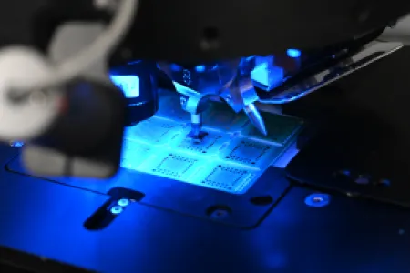
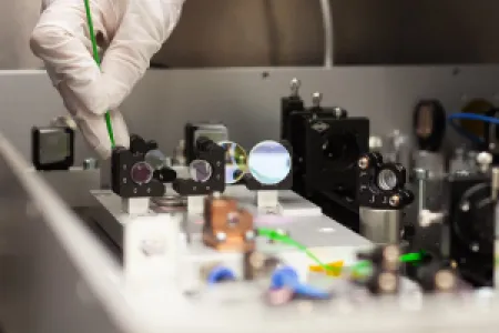
A photonic design only works outside the lab if its packaging holds alignment, manages heat and protects sensitive parts. AMS Technologies packages photonics on two scales. In Hanover, Germany, our team builds macrophotonic assemblies such as optomechanical modules and laser systems, including adjustment, calibration and testing in a cleanroom. In Paignton, UK, our business unit Bay Photonics packages microphotonic devices such as PICs, laser diodes, sensors and detectors. Capabilities include die and wire bonding, fiber alignment and coupling, hermetic sealing and seam welding, with micron-level alignment in manual to fully automated processes. Both sites take projects from prototype to high-mix, low-volume production.
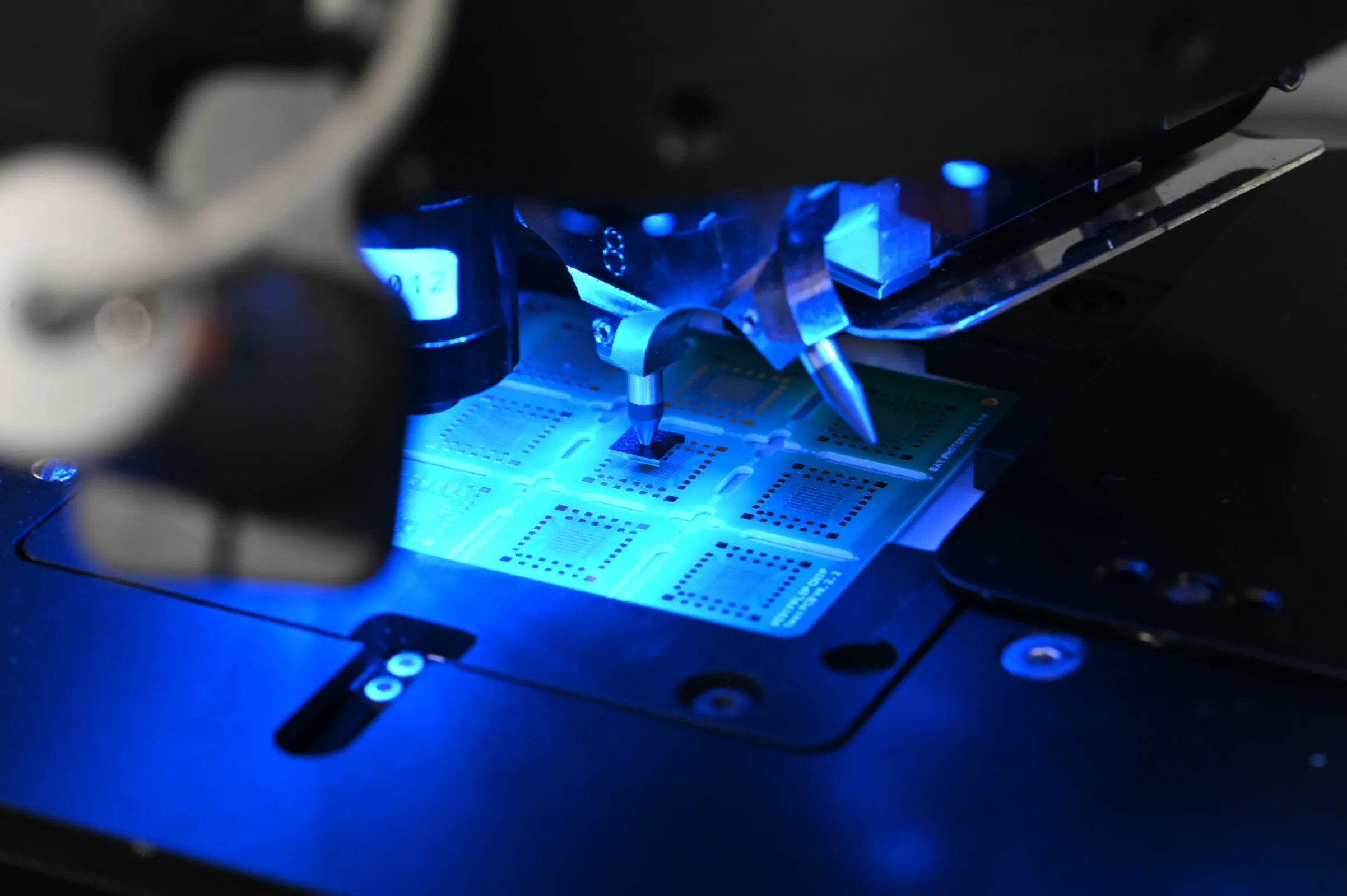
Microphotonics Packaging