3D-Micromac AG
About us
As a specialist in laser micromachining, we provide high-quality, reliable, and user-friendly laser systems for applications in semiconductors, glass & display, photovoltaics, microdiagnostics, and medical technology. Our solutions boost production efficiency, optimize processes, and reduce costs.
With 25 years of expertise, we support our customers as a trusted partner in process development, contract manufacturing, and development of tailored laser systems – with deep know-how in excimer and ultra-short pulse lasers and roll-to-roll processing of flexible materials.
From process design and system selection to commissioning and service – we’re with you every step of the way.
Address
Technologie-Campus 8
09126 Chemnitz
Germany
E-mail: info@3d-micromac.com
Phone: +49 371 400430
Internet: 3d-micromac.com
780 Montague Expy #306
CA 95131 San Jose
United States
E-mail: c.wolf@3d-micromac.com
Phone: +1 408 858 0107
Internet: 3d-micromac.com/
Contact person:
Christian Wolf
Director, Business Development & Operations | General Manager
E-mail: c.wolf@3d-micromac.com
Phone: +1 408 8580107
Joshua Stearns
GM Sales & Business Development US East
E-mail: stearns@3d-micromac.com
Phone: +1 603 3054263
Products & Services
We develop: Laser Processes and Manufacturing Technologies for the Products of Tomorrow
The technologies that will define the next decade are being designed today. We turn these ideas into manufacturable solutions by combining process expertise with in-house machine engineering.
Our laser contract manufacturing division develops customer-specific laser processes and manufactures components for small and large series. All production runs exclusively on 3D-Micromac laser machines. Our laser application center offers industrial systems as well as versatile development tools. We combine our know-how with beam sources from leading laser manufacturers to produce high-quality components and devices.
Production efficiency and cost awareness are our top priorities. We offer framework agreements for part manufacturing and, when production moves in-house, we build a laser system tailored to your requirements.
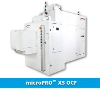
microPRO XS OCF: Laser Annealing for SiC Power Devices
Selective laser annealing enables targeted activation of functional layers with minimal thermal impact on surrounding structures – a key technology in advanced semiconductor production. Our systems offer outstanding process uniformity, repeatability, and efficiency at an industrial scale.
The microPRO XS OCF enables accurate activation of ohmic contacts on SiC wafers for power device applications. It delivers application-optimized annealing at the highest technological level while keeping CoO low.
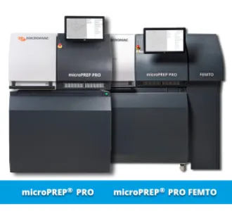
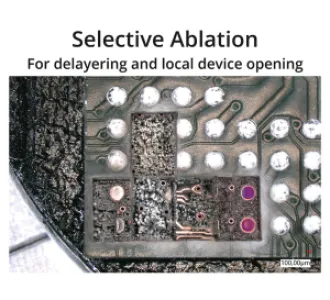
microPREP® PRO Systems: Laser-based Sample Preparation for Material Characterization
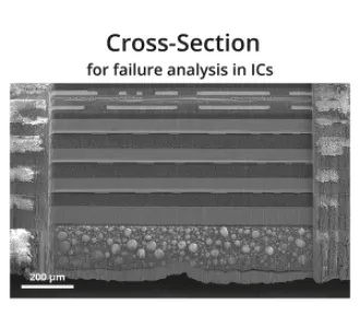
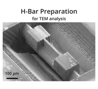
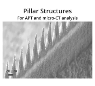
Failure analysis depends on well-prepared samples, and preparation is often the bottleneck. High-value FIB and SEM systems should spend their time on imaging and analysis, not on tasks a laser can handle faster.
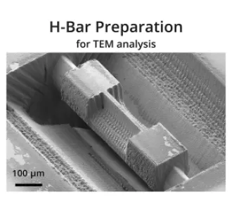
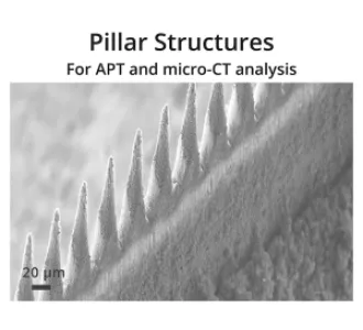
microPREP® PRO and microPREP® PRO FEMTO are dedicated systems for laser-based sample preparation. Both accelerate preparation for failure analysis methods, including TEM, SEM, APT, xCT, XRM, and micromechanical testing. As stand-alone laser tools, they can feed multiple ion-beam-milling and analysis tools simultaneously, so one system keeps several instruments productive.
microPREP® PRO uses a picosecond laser. microPREP® PRO FEMTO uses a femtosecond laser and extends this capability to challenging materials, including brittle, transparent, and stacked materials, as well as ceramics and polymers.
Both systems draw on almost 25 years of laser expertise. They have been field-proven for more than ten years and are continuously enhanced with user feedback, so they reflect the practical requirements of laboratory workflows.
Free your FIB/SEM for what it does best. Speed up your time-to-sample with laser-based sample preparation with microPREP® PRO or microPREP® PRO FEMTO.
microVEGA® xMR: Selective Laser Annealing for Monolithically Integrated GMR and TMR Sensors
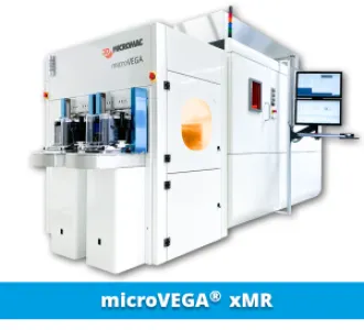
Selective laser annealing defines sensor sensitivity directly at wafer level. 3D-Micromac’s microVEGA® xMR combines a selective laser spot with a local, in-situ rotatable magnetic field. The laser heats defined sensor areas, and the magnetic field pins their reference layer in the desired direction. The heat-affected zone extends only a few micrometers beyond the sensor, so individual sensors can be placed closer to one another and to logic elements. This enables compact, monolithically integrated layouts, from Wheatstone bridges to angle and multi-axis concepts.
The microVEGA xMR supports both GMR and TMR sensors, with in- and out-of-plane programming. Laser pulse energy, magnetic orientation, and sensor dimensions are flexibly controlled by recipe, and very high energy homogeneity supports consistent sensor quality. Wafers up to 300 mm are supported, with an optional bridge-tool capability.
Proven in 24/7 high-volume fabs worldwide, the system turns complex sensor programming into a single, adjustable production step. Whether you are developing next-generation sensor architectures or scaling to series production, microVEGA xMR is built for cost-efficient, high-yield manufacturing.
Visit us at Photonics West 2027 on the German Pavilion to discuss your requirements for next-generation TMR/GMR sensor architectures.
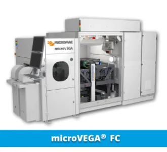
microVEGA FC: Ensuring fail-safe integrity and long-term robustness of analog, power-management & mixed signal ICs through permanent hardware configuration
Laser Link Trimming (LLT) enables permanent hardware configuration for analog, power-management and mixed-signal ICs in automotive, industrial, aerospace and other high-reliability applications. Typical devices include gate drivers, BMS ICs and high-side switches, where LLT supports variant configuration and permanent hardware limits for safety-critical and fail-safe functions.
Complementing rewritable NVM, Trim-DACs and electrically programmed OTP solutions, LLT creates irreversible, tamper-resistant configurations by modifying predefined metal links – without electrical programming stress or the need for dedicated memory structures.
3D-Micromac's microVEGA™ FC enables high-throughput wafer-level LLT on a production-grade platform for semiconductor manufacturing, combining ±200 nm positioning accuracy (3σ), closed-loop process control and on-the-fly processing at up to 400 mm/s for an exceptional balance of speed, precision and process stability.
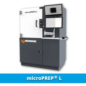
microPREP®L: Laser-Based Sample Preparation on Full-Wafer- and Board-Level
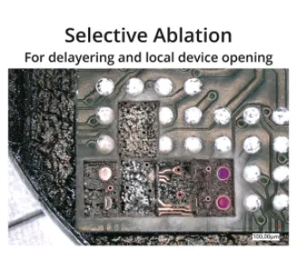
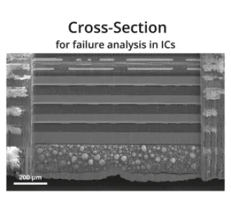
Our field-proven microPREP® systems accelerate sample preparation for a wide range of failure analysis methods, including TEM, SEM, APT, XRM, and micromechanical testing. The latest development, the microPREP® L, can prepare specimens on bigger samples like 12” wafers or system-level boards. These can even be prepared across multiple areas of the same sample in a single run, without process restarts.
Free your FIB/SEM for what it does best – speed up your time-to-sample with laser-based sample preparation with microPREP® systems.
microPOLAR™: Precision Laser Cutting for High-Index AR Waveguides
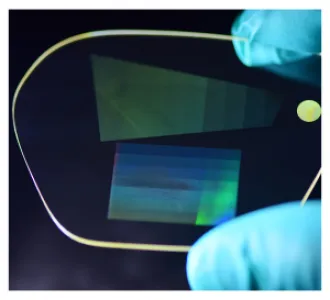
Augmented reality waveguides demand glass that is both optically precise and mechanically robust. 3D-Micromac's microPOLAR™ meets this challenge with a laser cutting process developed specifically for high-refractive-index wafers. It avoids edge damage, chipping, and particle formation while delivering high bending strength after singulation. Whether you are moving from prototypes to pilot lines or ramping up to mass production, the modular platform grows with your requirements.
Start with a flexible R&D configuration and upgrade in the field to additional process modules, automated handling, and quality inspection for volume production. microPOLAR supports leading high-index glasses, including SCHOTT RealView®, HOYA, and Corning, and integrates easily into production lines. Its small footprint and laser class 1 housing make it practical for both laboratories and production floors. Protect your investment with a system designed to adapt as your technology evolves.
Visit us at Photonics West 2027 on the German Pavilion to learn more about microPOLAR™ and discuss your AR waveguide cutting requirements.
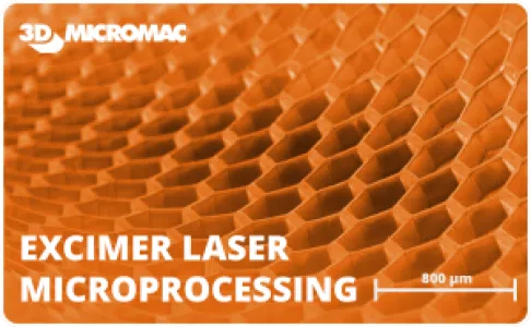
Excimer Microprocessing – from Idea to Series Production
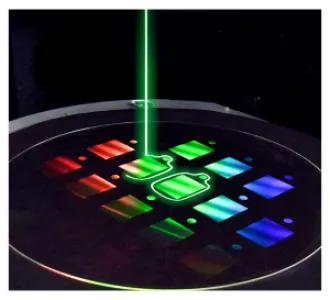
Whether thin-film ablation, microstructuring, lift-off for microLEDs, membrane thinning, or via-hole arrays – our excimer systems (157–308 nm wavelengths) enable high-precision processing using mask projection and line beam techniques. Our maximum duty-cycle solutions stand out for excellent beam shaping, high precision, and flexible process control, making them ideal for demanding industrial and research applications. They are used worldwide, e.g., in the display, semiconductor, medical, and sensor industries. In our application lab, we work closely with customers to develop tailored processes, produce prototypes, and provide series production when needed. That is how we create customized machine solutions for industrial microprocessing.
We look forward to discussing your requirements!
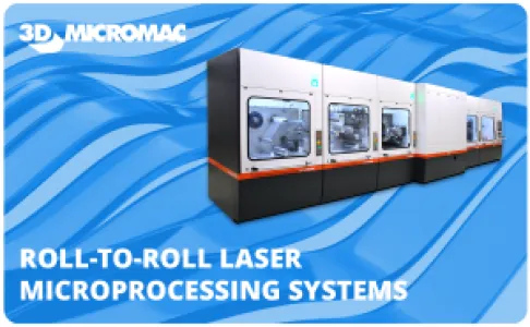
microFLEX®: Roll-to-Roll Laser Processing for Flexible Materials
Roll-to-roll production demands high throughput on wide webs without compromising precision. 3D-Micromac’s microFLEX® delivers both. The versatile roll-to-roll laser systems process polymer films, metal foils, and thin glass, making them an all-in-one solution for manufacturing flexible thin films in photovoltaics, electronics, medical devices, displays, and semiconductors.
For the photovoltaics market, microFLEX PV can make P1, P2, P3, and P4/PT isolation cuts on web widths up to 1.4 m. It supports CIS, CIGS, perovskite, and organic PV, with picosecond, femtosecond, and fiber laser sources for front- and backside ablation. Contactless web guiding and in-situ optical inspection keep the process stable, while dynamic process adjustment supports consistent quality.
The modular concept of 3D-Micromac’s microFLEX systems covers everything from applied research and pilot lines to 24/7 industrial mass production. Systems can run stand-alone or integrate inline, with MES connectivity via OPC or SECS/GEM. Customized configurations address specific process requirements, so your line can grow with your product roadmap.
Visit us at Photonics West 2027 on the German Pavilion to discuss your roll-to-roll laser processing requirements.
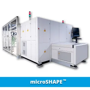
microSHAPE™: Versatile Laser Processing for Large Substrates
Large, flat substrates often require several tools and process steps. 3D-Micromac's microSHAPE™ brings them together on one highly versatile laser platform. Its gantry design scales in size and accuracy to match your process, from GEN 4 (680 × 880 mm) up to GEN 8.5 (2,200 × 2,500 mm) substrates, with thicknesses from 0.03 to 10 mm.
microSHAPE handles glass cutting, including display, cover, and ultra-thin glass, as well as thin-film ablation, volume ablation, and surface marking. It processes glass, metals, polymers, ceramics, display stacks, and coated substrates. Up to three laser sources and three beam paths let you combine processes in a single machine, and parallel working heads raise throughput.
From manual loading to robotic handling and full line integration, the system adapts to your production environment. Its modular design makes it a practical choice from first trials to series production.
Visit us at Photonics West 2027 on the German Pavilion to discuss your large-substrate laser processing requirements.
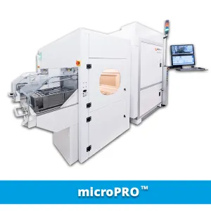
microPRO™: One Laser Platform for Virtually Every Micromachining Application
Micromachining requirements vary widely, from cutting and drilling to engraving, structuring, and laser lift-off. microPRO™ brings these applications onto one adaptable platform. Configuration packages combine technology modules such as high-speed cutting, drilling, engraving, structuring and modification, cylindrical machining, and laser lift-off, so the system is tailored to your process.
The platform processes metals, alloys, transparent and biological substrates, ceramics, and thin-film compound systems. You can choose one laser source from ns, fiber, fs, ps, or CO2 options, and different optical setups and quick-change clamping units adapt the system to each application.
The industrial microPRO offers ±0.003 mm positioning accuracy and substrates up to 400 × 400 mm. For compact applications, microPRO XS provides a freely configurable working area on substrates up to 200 × 200 mm, with ±0.015 mm positioning accuracy in a smaller footprint. Both systems support automatic handling, and loading and unloading can be designed to your production requirements.
Designed for research, development, and industrial production, the microPRO family scales from prototypes to production lines.
Visit us at Photonics West 2027 on the German Pavilion to discuss your micromachining requirements.