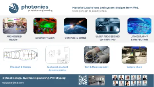
Photonics Precision Engineering GmbH
Booth number: 4205-31
ppe-jena.com
About us
Photonics Precision Engineering GmbH is s a young and dynamic photonics company based in Jena, Germany.
We are a team of international optical experts supporting you in optical design, tolerancing, system engineering, and project management.
With our industrial experience in the application fields of the semiconductor industry, microscopy, laser material processing, and AR/VR/MR, we accompany our customers from concept to manufacturing of their products and act as a long-term development partner.


Address
Moritz-von-Rohr-Str. 1a
07745 Jena
Germany
E-mail: info@ppe-jena.com
Phone: +49 163 3804277
Internet: ppe-jena.com
Contact person:
Products & Services
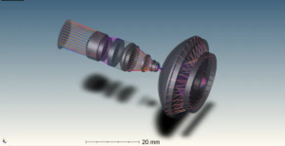
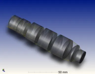
Optical Design
Optical System Engineering
Optical Engineering & Metrology
Physical optics modelling (e.g. RCWA, FDTD)
Supply chain management (from concept to pre-series)
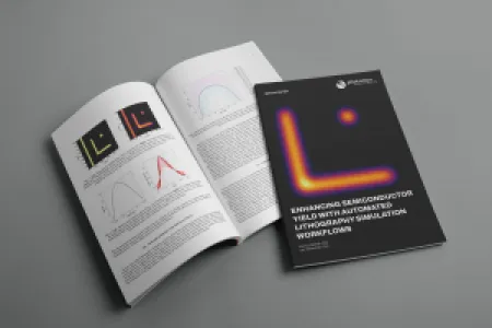
White Paper: Enhancing Semiconductor Yield with Automated Lithography Simulation Workflows
In the rapidly evolving field of semiconductor manufacturing, precise and efficient lithography simulations are crucial for achieving maximum production yield. This white paper demonstrates our expertise in conducting lithography simulations, focusing on key quantities such as aerial images, critical dimensions, bossung plots, process windows, and Normalized Image Log-Slope (NILS). By leveraging a commercial lithography simulation software....