PHOTONICPARTS
Booth number: 4205-04
www.photonicparts.com
About us
PHOTONICPARTS, a brand of XCCES GmbH, specializes in advanced joining and assembly technologies for high-performance photonic components. The company designs and manufactures customized soldered assemblies such as laser crystal packages, non-linear crystal packages, and optical submounts that ensure maximum thermal stability and long-term reliability.
Its core expertise lies in the flux-free production of homogeneous, large-area solder joints for virtually any material combination — achieving outstanding thermal and electrical conductivity, mechanical robustness, and vacuum compatibility.
PHOTONICPARTS supports customers in laser packaging, precision alignment, and thermal management for applications in laser technology, aerospace, defense, and quantum systems. Combining deep materials expertise with advanced process engineering, the company delivers scalable and reproducible joining solutions for next-generation photonic assemblies.


Address
Ericsson-Allee 1
52134 Herzogenrath
Germany
E-mail: phillip.dittmann@xcces.de
Phone: +49 2407 5023350
Internet: www.photonicparts.com
Contact person:
Products & Services
Precision joining for photonic excellence
At PHOTONICPARTS, we specialize in high-performance packaging and assembly solutions for laser and photonic components. Our core expertise lies in flux-free-vacuum soldering, packaging technologies, robust thermal management, and hermetic sealing technologies. From laser crystal packaging to complex optics and subsystems for quantum, we integrate optical elements in a reliable and scalable manner thanks to our advanced joining processes. Whether it’s for highpower laser cooling, quantum applications, or aerospace-grade components – our solutions are made to last and withstand harsh environments.
Our technology
Flux-free vacuum soldering for optical, metallic & ceramic components
Active surface preparation: Applying of solderable metallization of nearly all materials
Low-melting solders tailored to thermal & mechanical needs
Thin-film to thick-layer solder deposition via PVD technology
Robust bonding layers with excellent thermal and mechanical stability
Stress-optimized joints – ideal for laser cooling, vacuum and immersion optics
Hybrid assemblies with electrical, optical and fluidic interfaces
Packaging solutions from lab-scale/ demonstrators to industrial series integration
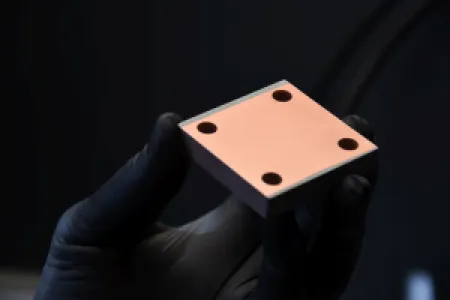
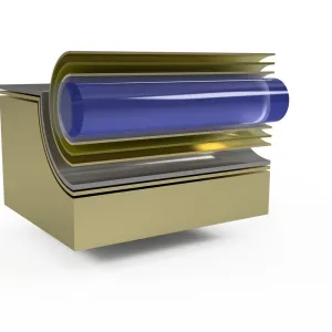
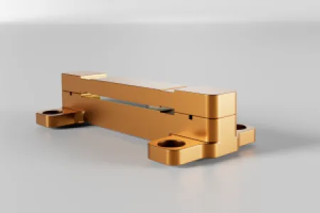
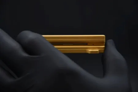
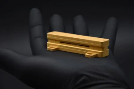
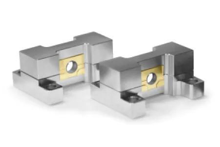
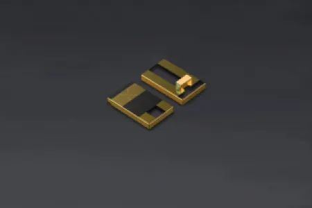
LCP-S (Slab Crystal Package)
Fully soldered laser high power crystal package for slab geometries.
Excellent performance for amplification of ultrashortpulse laser beams.
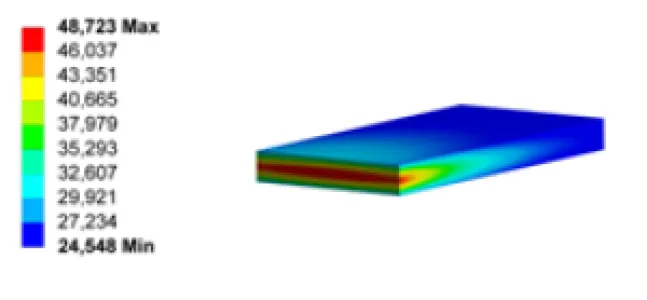
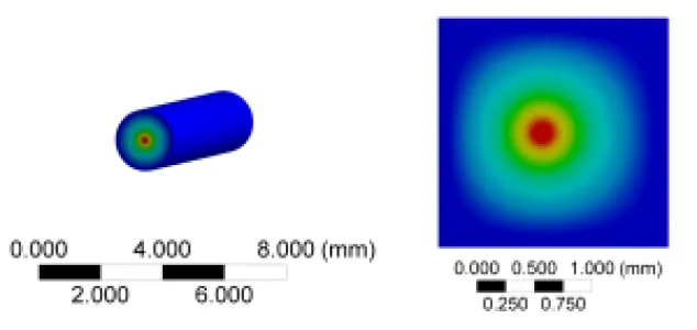
Depending on the setup and applied power, thermal bonding of solid-state laser crystals plays a key role in achieving stable and high-performance amplification power. Our design concept and solder joining technology enables us to achieve a homogeneous heat dissipation over large bonding surface areas. After years of dedicated research and development for high-end laser beam sources supported by thermal simulations, we have innovated a distinctive approach for mounting and cooling solid-state laser crystals.
Stress-reduced crystal mounting due to CTE-matched heatsink material pairing
Flux-free soldered crystal package
Homogenous heat dissipation over entire crystal surface area
Design and manufacturing of packaging solutions for laser gain media
Industry proven concept
Excellent performance for demanding industry and laboratory application
Easy adaptable to different crystal dimensions and dopant concentration
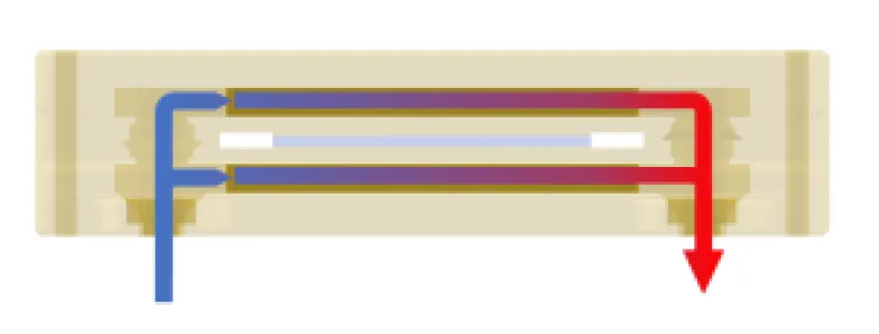
Integrated water-cooling with optimized in-flow through microchannels
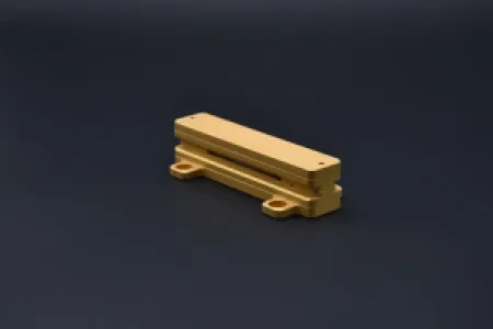

LCP-R (Rod Crystal Package)
Fully soldered laser high power crystal package for rod geometries.
Excellent performance for amplification of laser beams.
Depending on the setup and applied power, thermal bonding of solid-state laser crystals plays a key role in achieving stable and high-performance amplification power. Our design concept and solder joining technology enables us to achieve a homogeneous heat dissipation over large bonding surface areas. After years of dedicated research and development for high-end laser beam sources supported by thermal simulations, we have innovated a distinctive approach for mounting and cooling solid-state laser crystals.
Stress-reduced crystal mounting due to CTE-matched heatsink material pairing (submount technology)
Flux-free soldered crystal package
Homogenous heat dissipation over entire crystal surface area
Design and manufacturing of packaging solutions for laser gain media
Industry proven concept
Excellent performance for demanding industry and laboratory application
Easy adaptable to different crystal dimensions and dopant concentration
Integrated water-cooling with optimized in-flow through microchannels


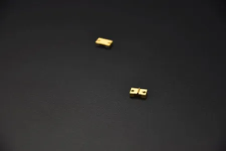
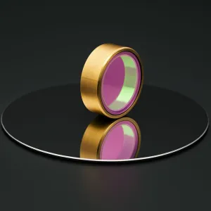
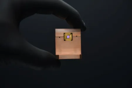
NLCP (Non-linear Crystal Package)
Non-linear crystral packaging – frequency conversion units
Our non-linear conversion chambers are fully outgassing-free, making them ideal for UV applications with minimized aging. The non-linear crystals are soldered onto CTE-matched submounts, ensuring mechanical stability and thermal reliability. Hermetically sealed or purgeable designs, combined with a precision, provide maximum protection against contamination and optimal thermal performance.
CTE-matched heatsink material pairing for NL-crystals
Including high precision resistance heater
Sealed box to prevent contamination and to extend lifetime
Fully vacuum compatible
purging option available
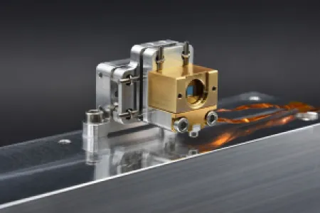
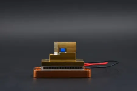
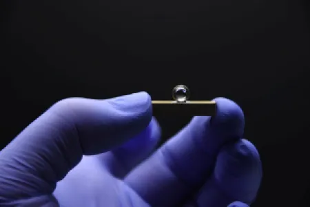
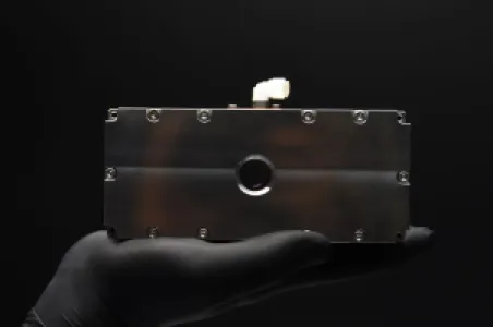
FA-I/R (High Power Faraday Isolators / Rotators)
Optimized for multi-100W to kW laser systems
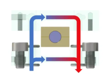
Our Faraday rotators and isolators are designed for laser systems operating in the multi-100 W to kW power range at 1030 nm and 1064 nm. A key feature is the direct soldered connection of the crystal barrel surface (KTF or TGG) to a water-cooled heatsink, realized using a flux-free soldering process. This enables highly efficient thermal management and minimal thermal shift, even at highest optical loads. Thanks to our proprietary magnetic field design and the use of soldering technology, we offer stable, high-performance solutions for applications where standard components are no longer sufficient.
Soldered KTF crystals with integrated water cooling
Slab and rod crystal geometries
Power rating: Multi - 100W to kW
max Aperture: Rod (dia 15mm / slab 15x25 mm²)
Crystal material: TGG/KTF
Wavelength: 1030 nm / 1064 nm
Transmission: > 95% Extinction ratio: > 30 dB
Damage threshold: 10J/cm² at 10 ns, 1J/cm² at 8 ps


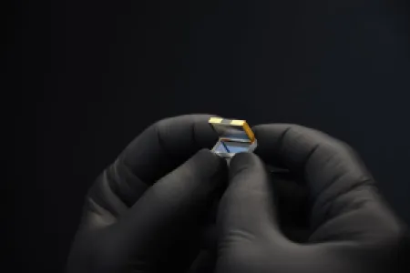
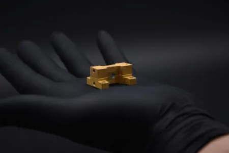
Optics on Submount / Metallization / Optomechanics / Active Alignment
Robust optomechanics and optics on submounts
By utilizing flux-free soldering and CTE-matched submounts, our optomechanical assemblies enable low-stress mounting of optical components, ensuring long-term stability and high optical quality. This approach is particularly suited for deformation-sensitive elements, such as thin optical plates where wavefront planarity must be preserved. Additionally, the soldered, adhesive-free interfaces offer minimal outgassing, making them ideal for UV applications and contamination-sensitive environments. Our modular design allows for straightforward adaptation to different optic sizes and geometries.
Metallization service for optics, ceramics, metals
Application of solderable metallizations
partial metallization of optics
PVD application of different solder materials
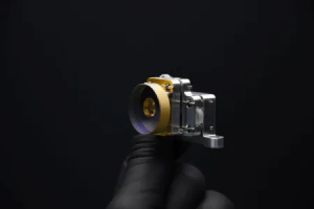
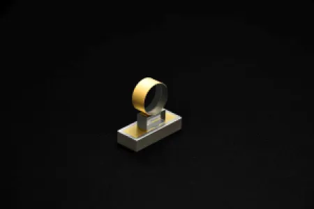
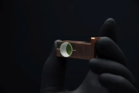
High precision flexure mirror mounts with soldered CTE-matched optic interface
Our SFM mirror mounts feature monolithic bodies with optics soldered via CTE-matched submounts for maximum mechanical and thermal stability. The flux-free soldering process ensures stress-free, long-term reliable bonding without adhesives. This design enables robust, vibration-resistant alignment – ideal for high-stability beam delivery in demanding environments.
Excellent pointing stability over changing conditions (Very low angle change (<20μrad in both axis) after multiple ΔT=60K temperature cycles
Optical component soldered on CTE-matched submount to reduce thermomechanical stress
Ultra compact design; minimal footprint
Vacuum compatible
Easily adaptable to different mirror dimensions
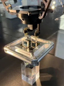
Optical components for machine-assisted assembly
Our active alignment technology enables us to achieve repeatable, consistent positioning of optical components in a molten solder interface. Local remelting using integrated heaters allows us to fix optical elements permanently and, stress-free fixation – without raditional mounts. The result: compact, robust, and precisely aligned optical systems.
Repeatedly adjustable in liquid solder
Fully integratable in machine-assisted automation setups
Completely glue-free, UV/vacuum/spacecompatibility
Integrated heater and temperature sensor